Memories
Digital IC design and vlsi notes
Memories
- Source this playlist on memories.
Introduction
- Memories are large storage devices
- Other storage devices like latches (level sensetive) and registers (edge sensetive)
- Memories are mass storage devices, arrat structures of identical elements that are repeated
- Memories have two main concerns density and speed
- For random logic the cost of silicon area is generally small, and the trend has been for silicon area to be cheaper and cheaper
- But for memories we want to cram as much storage as possible in a small area and therefore density matters alot
Time-sharing
- It’s a phenomenon that we have to deal with because processing units are becoming very fast (faster than we need to)
- Assume processing units that have a throughput more than needed (produces output faster than needed)
- we can underclock all processing units and get the throughput needed
- we can use half the number of processing units, in the first cycle provide the input of the first half, the second cycle provide the inputs of the second half
- This is called time-sharing and it will provide the required throughput
- The problem with time-sharing is at some point you are gonna have alot of intermediate data to store
- the immediate instinct is to store them in a register
- but if you imagine having many of the processing units and parallel inputs and outputs then this becomes a takes that requires a mass storage device (memory)

Memories
- The problem with digital design is always how to figure how many memory banks needed
- Because memories tend to be faster than processsing units so they can provide inputs and outputs multiple times per each processnig unit cycle
- Some time that’s not even enough and you need to divide the memory into multiple banks
- Memories and their bandwidth are significantly important even more important than the frequency of operation of random logic
- you need to pay attention not only to the amount of data you can store in the memory but also to how fast you can read and write this data
Memory Classification
- Roms (read-only memories) A memory that could only be written a signle time
- Nor roms
- NAND roms
- They form nor and nand dynamic logic gates in the memory columns
- NVM (Non-volatile memories) Memories whos contents gonna stay there wether there is a power supply or not, and they are also rewritable in a way (programability)
- RAM SRAM and DRAM
- Storage mechanisim
- Dynamic nodes: storing on a capacitor
- Static nodes: based on positive feed back and pairs of inverters
- NVMs and ROMs don’t store on capacitive node or a positive feedback loop, they store or don’t sotre based on the presence of lack of a transistor
- Dynamic reading means that memories form dynamic gates along the columns
- Some of these memories can be created using standard cmos, some of them need weird things to happen inorder for them to be implemented
- Memories that cann’t be embedded in an ASIC operation either require a very difficult process that involves non std cmos combined with std cmos or will be off chip memory
- Effictive roms are very difficult to embed
- Efficient DRAMs need special processing and often uesd as off chip main memories in micro processors
- SRAMs can be embedded using std cmos and it’s what we mean when we say memories when we design digital circuits, its disadvantage is that it’s huge, a signle SRAM cell is bigger than a signle cell of any other memory type

Memory array architecture
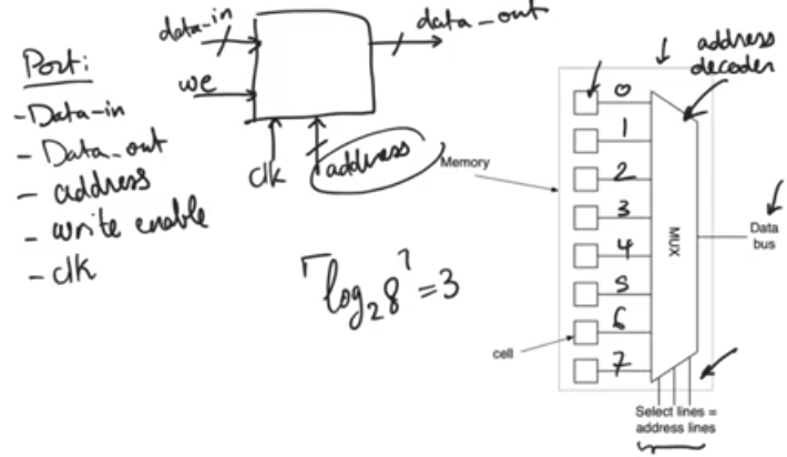
Memory port
- A memory is a collection of storage locations that share a signle port or multiple ports in some cases
- A port is a collection of buses that cab be used to access the memory locations, A single port will contain:
- Data-in bus, Data-out bus, address bus
- write-en to tell wethere we are reading or writing to the address indicated by the address bus
- clock (optional) because some memories are asynchronous, but most practical memories are synchronous
- A collection of all these buses is called a port
- Address bus cannot be absent for a port, ports are distinguished by address bus, how many address buses we have determines how many ports we have
- memory locations can be multiple bit locations as long as they are all storing the same number of bits and its size is the same as the data bus
Multi-port memory
- A two port memory contains two address buses, this allows us to read from two independant memory locations simultaneously
- Address bus indicates that there is an indenpendant address decoder dedicated to it
- In a read-write memory you can have multiple ports and some of them might be read-only, write-only or read-write as long as you have an independant address decoder for each of the independant ports
- This way of arranging the memory core (the memory locations) is extremly inefficient cause it’s a linear memory array
- because typical memory is not 8 bits long, it’s millions of bits and words long.
- so for a large memroy it’s gonna have a very strange aspect ratio, it’s gonna be much much longer than it’s wide
- This is gonna make its layout a nightmare and gonna make the chip more expensive for no reason at all

Square arrays
- Practical memories are square arrays instead of a linear array
- Vertical wires are called bit lines
- Horizontal wires are called word lines
- At the intersection of every bit line and word line you’ll find a cell that contain a zero or a one
- If we have
2^m bit lines and 2^k word lines
- this memory contains
2^kx2^m locations = 2^(k+m) bit memory
- word lines can be decoded using k*2^k row decoders
- bit lines can be decoded using 2^m*1 column decoders
- A reading operation is started by providing an address of k+m bits
- k bits to the row decoder
- m bits to the column decoder
- The row decoder decodes the
k bits and decide which row of the 2^k we want to access and enable it, so outputs will be available on m bit lines
- so the column decoder (A multiplixer) that takes a
2^m bit lines and produces a single output line depending on the m bits of the address
- Array elements
- the core (array of cells)
- row and column decoders
- sense amplifier
- buffers
- Buffers are used in read-write memories to drive the values of the column decoder to specific values when writing
- Sense amplifiers resolve a fundamental contradiction about the cell design
- we need cells to be small because density is really important to memories
- if a cell is a small, it has a reduced ability to drive the huge capacitance of the columns or the bit lines, and speed it also important for the memories
- sense amplifier help reduce this conflict

Practical memories
- Consists of multiple square arrays called cores
- These multiple arrays can then have one more level of multiplexing and decoding between them called the bank selection level
- Delay of memories is more or less contingent on the length of the columns and the rows
- In practical arrays it helps to divide them into smaller arrays to keep the length of the word lines and bit lines limited
