DRAM
Digital IC design and vlsi notes
DRAM
- Source this playlist on memories.
Introduction
- D refers to dynamic,
- It refers to the method of storage not the way data is read from cells
- because all memory arrays are gonna read using precharge transistors,
- and gonna have high impedance nodes while reading
- Storage mechanism is dynamic, we rely on high impedance capacitive nodes to store values
- We are opening our selves up to problems of leakage, charge sharing,
- All the signal integrity issues in dynamic cmos logic
- These effects have a much more determintal impact on drams than they do in random dynamic cmos logic
- The main thing about drams is their density
- Mass storage in a small area
- really slow compared to srams
- NAND flash roms compete with drams in terms of density but they have issues in reading and writing speed
- DRAMS is the memory of choice for mass storage in microprocessors where sram forms on chip caches
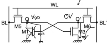
Four transistor DRAM cell
- Formed by taking an sram cell and removing the pmos transistors
- removed M2 and M4 from sram cell and left the two nmos transistors of the static inverters and the two access transistors
- storing a one at node Q
VQ=VDD, causes node Q’ to be zero volt VQ'=0
- When the access transistors M5,M6 are off the cell will keep its state
- because node Q is at Vdd turns M3 on causing Q’ (drain of M3) to be connected to ground 0v
- because Q’ is at 0 volt M1 is cut off which allows node to keep the value of VDD
- Node Q is storing the value dynamically,
- dynamic high impedance node storing Vdd.
- Q’ in this case is a low impedance node connected to ground
- To read from this cell, precharge the bit line and bit line bar to VDD
- Then enable the access transistors M5 and M6 using the word line
- BL’ is gonna charge through M6 and M3
- While BL is not gonna discharge because Q is also at Vdd
- Therefore Q and BL are at the same voltage, and M5 is cutoff
- Writing to the cell is by driving bit line and bit line bar to their correct values
- Less area than sram cells
Three transistor DRAM
- This is a practical dram cell, because the four transistor model had redundant transistor
- half the area of the sram cells
- Separate controls for reading and writing
- WE: write enable, RE: read enable
- writing through M5 and reading through M6.
- Bit line and bit line bar won’t be complements of each other, they aren’t working differentially
- one of them is the write line and the other is the read line
- To Write one to the cell
- Drive the write line to Vdd
- Then enable the write enable line (word line)
- This causes the capacitance at the storage node to charge up to Vdd
- Then we lower write enable
- Then this storage node becomes high impedance node because it observes a cutoff transistor M5 and a mosfet gate of M3 so it’ll keep the value of Vdd
- This value of Vdd at the storage node is gonna guarantee that M3 is always on
- To read
- precharge the read line to Vdd
- raise the read enable to one
- The Vdd on this read line is gonna discharge through M6 and M3
- M6 is on because read enable is one, and M3 is one because there is Vdd at the storage node
- so we are gonna read a zero volt (write Vdd read 0 inversion)
- if you stored zero, then transistor M3 is gonna be off,
- when you precharge the bit line and enable read enable
- the bit line won’t be able to discharge and it’ll remain at Vdd
- This is solidly a dram because storage takes place at the capacitance of a high impedance node
- The storage capacitance is a parastic capacitance of the drain of M5 and the gate of M3
- This is different then the one transistor dram cell which requires a specialized storage capacitor
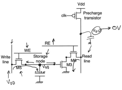
- The advantage of this to the smaller one transistor dram cell
- three transistor dram cell doesn’t need an explicit capacitor for storage, it just uses the parasitic capcitance
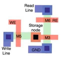
Layout
- We aren’t using any wierd processing steps
- we aren’t using any layers that doesn’t exist in standard cmos
- you can create three transistors dram cells using standard cmos, can be used as embedded memories on chip
- When you have embedded memories they usually happen to be srams
- This allows you to not think too much about the issues of leakage or charge sharing and -other dynamic circuits problems
- When dram cells is used it usually off chip as main memory in this case it’s better to use a one transistor dram cell
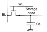
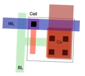
One transistor DRAM
- Dram is probably the most complicated memory to read from and to maintain
- The cell consists of a single access transistor
- storage takes place on the storage capacitor Cs
- single bit line and a signle word line
- To store a zero,
- set bit line to zero
- raise word line to Vdd so that the access transistor turns on
- the storage capacitro discharge and zero is stored
- When the word line is disabled, the zero volt is maintained on the storage capacitance Cs in a high impedance state
- To store Vdd
- Drive Vdd on the bit line, then enable the word line
- because the access transistor is nmos to promote density, the maximum storage value at the storage capacitor is
Vdd-Vth, to store Vdd, drive the word line to Vdd+Vth
- One transistor Drams uses dynamic read operation meaning that we precharge the bit line, and then enable the word line
- To read
- precharge the bit line, then enable the word line
- if Vdd is stored, then
Vout=Vdd is read on the bit line
- if zero is stored, then we have two capacitors at high impedance
- CBL contans Vdd obtained at precharge
- Cs contains zero volt obtained by previously being written two
- These two are connected together using the access transistor
- Charge sharing happens because the two transistors are in parallel with each other
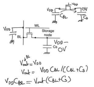
- if we are precharging the bit line to Vdd/2 then
- if the storage capacitor is storing Vd, the bit line shares with the storage capacitor and VBL is gonna increase a little bit
- if Cs is storing zero, the VBL is gonna decrease a little bit
- this has the advantage the we observe a change in both cases which helps in the design of the sense amplifier
Issues
- one transistor dram cells has destructive read
- When you read the value stored in a cell, you also destroy it, because you are taking away or giving to the charge on the storage capacitor Cs
- at the end of the charge sharing operation both Cs and CBL have the same value on them which is neither 0 or Vdd
- To have a meaningful memory, when you read you have to go back and rewrite the value again
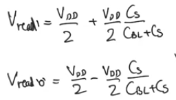
- The DeltaV observed on bit line is really small
- the difference between reading a one and reading a zero is
Vdd*Cs/(Cs+CBL)
- CBL is the capacitance of the eniter bit line and it’s also loaded by all the drains of all the access transistorsa
- Cs is a small capacitance
- We can’t relay on the parasitic capacitance of the access transistor to provide Cs cause in this case the DeltaV is imperceptible
- We have to use a physically created capacitor to provide enough storage to provide enough charge so that it has an impact on the bit line when reading
- For capacitance to increase we have to increase area of the capacitor plates this contradicts with DRAM density
Layout
- Layout that uses normal cmos layers
- diffusion bit line and metal word line (different from the others)
- the problem here is that we will use the polysilicon to create one plate of the capacitor
- this polysilicon is gonna run the entire length of the array (connected to ground)
- the other plate is diffusion layer shorted to the drain of the access transistor
- the problem here is that this is a non linear capacitor
- the capacitance because of the use of diffusion layer is non linear
- it’s really hard to manage
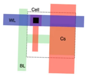
- To create a linear capacitor we use another polysilicon layer for the second plate
- one of them creates the bottom plate of the capacitor
- the other one is the normal poly layer which runs the length of the entire cell and connected to ground
- the bottom plate polylayer is gonna be shorted to the diffusion layer of the transistor drain by creating as many contacts as possible
- this storage capacitor needs to be as large as possible so when we do charge sharing it has as large an impact on the bit line voltage as possible
- this is done by increasing the cell area, which has a bad impact on the cell area and therefore density
- most practical drams comes in an independant chips, they aren’t integrated in the same chip as the system which allows them to do some nifty tricks
- Like creating the capacitor through a 3D strucutre to increase the area without increasing the foot print
DRAM read, write and refresh cycles
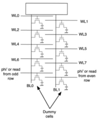
Dram array
- You have to use sense amplifiers
- While sense amplifiers help speedup other kinds of memories like srams
- For drams sense amplifiers are indispensable to reading
- because the dram cell itself isn’t capable of creating any kind of perceptible DeltaVBL
- sense amplifiers by definition are differential while drams are single ended
- The way to deal with this is to have two bit lines connected to each sense amplifier
- in each bit line we will have a dummy cell at the end of it
- if we are reading from the cell at the upper bit line we activate the dummy cell on the other side and viceversa
- the dummy cell might not contain anything it’s an empty cell, so when reading it’s not gonna change and remain at VDD/2 allowing us to read DeltaV
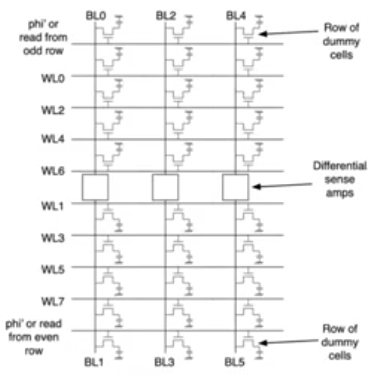
- In terms of layout the array is usually folded like this
- so that it’s exists on one side of the sense amplifier
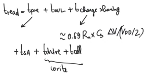
Write cycle
- Drive the value to be written on the bit line
- enable the word line
- wait for the cell to store the value driven
Twrite = Tdrive + Twordline + Tcell- Drive delay means that we are driving the bit line using drive buffer
- Delay of an inverter chain
- Word line delay can be calculated exactly the same way for rom array
- with one exception which is word lines in drams are made using metal layers
- which means that they can be modeled as a lumped capacitor, which makes calculation easier
- Cell delay the time it takes for the transistor to move the correct value to the storage capacitor
- single time constant RC circuit
T=RnCs resistance of the access transistor times the capacitance of the storage capacitor
Read cycle
- precharge the bit line, single time constant circuit with the capacitance of the bit line and the resistance of the precharge transistor
- Bit line now is in the diffusion layer, has a resistive component
- Enable the word line, word line delay same as write
- cell delay (charge sharing delay)
- charge sharing between the storage capacitor and the bit line capacitor
- Charge sharing time is pretty small because the amount of charge is small
- sense amplifier delay
- takes care of taking the charging sharing swing and maximizing it to full swing
- Once you read you have destroyed the value stored in the cell
- take the full swing values produced from the sense amplifiers
- route them to drive buffers (same used for writing)
- drive them on the bit line
- same delay of write operation
Refresh cycle
- Drams have severe signal integrety issues
- The stored value is stored in a capacitor
- it’s capacitance is relatively small
- A lot of different phenomena can affect the stored charge on this capacitor (takes away or adds to the charge, chaning the stored value)
- cosmic radiation tends to cause the value stored in DRAM cell to evaporate
- causing the dram cells to randomley lose their data
- which is why dram arrays are always used in conjunction with forward error correction
- Leakage charge flowing through the cut-off transistor because it doesn’t have infinite resistance
- With time the stored value is gonna evaporate
- it’s more an issue for dram then any other dynamic cmos circuit
- for other dynmaic cmos circuits like latches or registers their inputs are updated every cycle, they precharge and evaluate every cycle
- which is why you only need to make sure that the clock cycle isn’t too long to allow any impact
- With memories there is a danger that you might write somthing and won’t need it for a very long time depends on the program
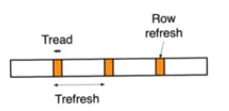
- This is why DRAMs have to refresh all of their stored data regularly
- refresh means reading the values and writing them again
- read cycles include rewrite at the end
- all we have to do is to do a read operation then it’s a refresh
- When you enable a specific word line, you will enable all the cells in the word line
- so you do refresh on a row by row basis
- The amount of time it takes to refresh one row is
Tread with m rows in the array,
- refresh rate depends on the amount of leakage
Ileak=Cs*DeltaV/DelatTDeltaT=Cs*DeltaV/Ileak the time it takes to leak DeltaV (toleratable leakage voltage amount)- This is the amount of time that can pass between two consecutive refreshs for each row
- The memory as a whole needs to do refesh so that each row observers DeltaT between two refreshes
Trefresh = DeltaT/m where m is the number of rows
- during the whole time
Trefresh every cell can do reading and writing normally
- but it’s wasting some time to do refresh, the time is a read time
- The overhead of refreshing is
Tread/Trefresh = Tread*m/DeltaT