Static hazards
Digital IC design and vlsi notes
Static hazards
- Source this playlist on Testing.
Static 1 hazards
- Identify static one hazards and solve them using K-map approach
- Static 1 hazards always reduce to the simple form of
- two paths that reconvene at an
OR gate
- and these two paths have to have differential delay
- and they have to present the
OR gate with some form of true and inverted form of a certain variable
- When that happens you’ll possibly see a static 1 hazard
- depending on the delays of the circuits and the inertial modle delay used
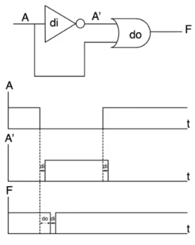
Example
- The previous form doesn’t have to be explicitly exist in a circuit to have a static 1 hazard
- it could be implicitly present
- The circuit in the example has a static 1 hazard
- Variable
A has two path to the final OR gate
- This isn’t enough for a static hazard to occur
- There also has to be an inversion between these two variables
- The inversion of
A happens using the NAND gates in the upper branch
- The third condition is that the two branches has differential delay so that you can have a time through which the glitch appears
- this is obvious in this circuit because the upper branch is much longer than the lower branch
- The values for other inputs to the circuit are the values that will cause the glitch to appear
- The glitch doesn’t appear in all conditions under all circumstances
- It only appears under certain conditions
Solution
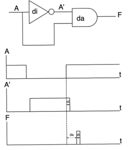
Combinational delay
- Static hazard occurs because we see a true and a complement form of a variable having differential delays
- The glitch occurs when the variable makes a transition and there is a period of time in the middle where neither of
A or A' are 1, thus we see a glitch with a value of 0
- If we compensate the differential delay by adding a delay to the lower path so that both paths’ delays are equal
- Then
A and A' are gonna match exactly
- If that happens, there is no space for the glitch to occur
- This delay has to be combinational delay
- Absolute time measured in terms on nano seconds
- It’s extermly difficult to match combinational delays, so it’ll be extermly difficult to match the delays of the branches exactly
- This approach isn’t very practical
K-map approach
- The correct approach is to add extra combinational logic which masks the offending transition
- Going back to the original circuit
F=AB'+BC
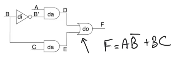
- The K-map has 8 squares each one represent the min terms
- The function has active min terms
3,4,5,7
- Static 1 hazard happens when
A=1 and C=1
- If be makes a transition between squares
5 and 7 the glitch happens
- for min terms
m5<->m7 we have a glitch where the only variable changes is B
- these min terms are adjacent and not covered by a group
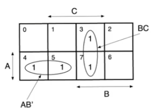
- The solution is to cover these min terms by a group
- This additional term is
AC
- This is a redudant covering that doesn’t change the logic function
- It’s additional hardware that will solve the static 1 hazard and completely mask it
- In the original problem when we make a transition between min terms
m5<->m7 the function is supposed to keep F=1
- in
m5 we are relying on the term AB' to maintain the value of 1
- in
m7 we are relying on the term AC to maintain the value of 1
- But
C and A aren’t the variables that give us the 1 at the nodes D and E, B and B' are
- because there is a differential delay between
B and B' then there will be a period of time where neither B nor B' are ones and therefor you’ll see a glitch
- When adding the term
AC we now have a term where when both A and C equal to 1 this term is also 1
Static 0 hazards
- similar to static 1 hazards in terms of structure and solution
- Static 0 hazards reduce to the simple form of
- two paths that reconvene at an
AND gate
- and these two paths have to have differential delay
- and they have to present the
AND gate with some form of true and inverted form of a certain variable
- Variable
A made two transisitions 1->0 and 0->1, the glitch only appeared when it made a transition from 0->1
Example
- The previous form doesn’t have to be explicitly exist in a circuit to have a static 1 hazard
- Variable
A has two path to the final AND gate
- The inversion of
A happens using the NAND gates in the upper branch
- There is a differential delay between the bottom and the top branches because the upper branch is much longer than the lower branch
- The values for other inputs to the circuit are the values that will cause the glitch to appear
- The glitch doesn’t appear in all conditions under all circumstances
- It only appears under certain conditions
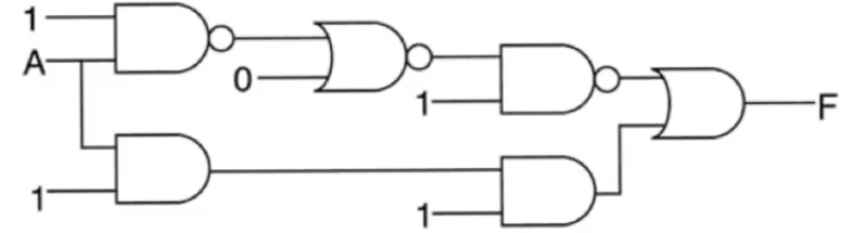
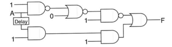
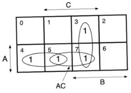
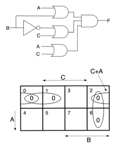
Kmap approach
- This is a POS (product of sums) circuit, the variable which will cause the static hazard is variable
B
- The output is
F=(A+B)(C+B') which allows us to observe a glitch if B makes a transition 0->1
- For POS circuits when you suspect there is a static 0 hazard, it’s better to represent the circuit on the Kmap using zeros rather than one
- circuit represented using max terms
- The active max terms are
m0,m1,m2,m6
- The glitch happens at two adjacent
0 squares which are not covered by a group
- The kmap has adjacency on the edges
- Sqaure
m2 and m0 are adjacent
- any transition between them represent a glitch
- The only variable that makes a transition between them is
B
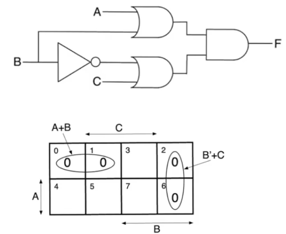
- This problem is solved by covering the uncovered transition with a redundant term
C+A
Static hazards in logic equations
- The kmap approach towards detecting and solving static hazards is very limiting
- it doesn’t give any way to deal with dynamic hazards
- it only allows you to deal with functions with up to four variables
- The best way to detect and solve hazards static or dynamic is to look at logic expressions and try to work from them
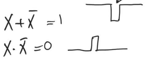
- When you are looking at an equation you are looking for an expression in the form
X+X' or X.X'
- These are terms that indicates the possibility of a hazard
X+X' is always equal to 1 and because there could be a differential delay between the X and X' there is a possibility that there will be a glitch (static 1 hazard)X.X' is always equal to 0 and because there could be a differential delay between the X and X' there is a possibility that there will be a glitch (static 0 hazard)
Example
- Function
Z=AB(C+DE')+F(GH+EK)
- In this expression the only variable that has the potential to have a hazard is variable
E
- as it’s the only variable that makes an appearance in its true and complement form
- We need to know what other variables’ values brings up the glitch to know whether it’s a static 0 or 1 hazard
- We have to think what they have to be at inorder to allow
E and E' to meet together
- All variables that are multiplied (ANDed)
E or E' have to be 1 inorder to make it propagate A=B=F=K=D=1
- All variables that are added (ORed)
E or E' have to be 0 inorder to make it propagate C=0
G and H we need only on of them to be equal to 0- They can be
GH=0X or GH=X0
- In that case
Z=E'+E so we have a static 1 hazard
- To solve this glitch we add another product them that keeps the value of
Z at one in this condition
Z=AB(C+DE')+F(GH+EK)+ABFKDC'GH'- This additional term solves the static hazard
- there could be multiple sources of hazards in which case you will deal with each variable independently
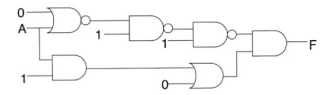
Static hazards in complex circuits
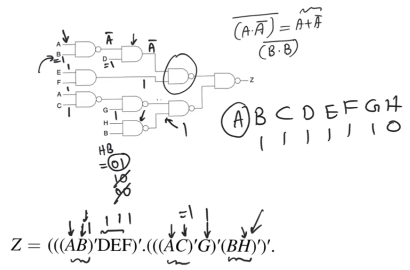
- for a static hazard to occur we have two at least two appearances for a variable
- All the input variables that have a single appearance don’t have a potential to cause a glitch
- In the example the only variables that could cause a glitch are
A and B cause they both appear twice
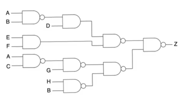
- For
A the gate in which both occurences appear is the final NAND gate, we have to check the other static hazard conditions
- The upper branch
A appearance passes through the first NAND gate to be A', then A' for the next AND gate, then it’ll make an appearance as A after the second NAND gate
- The bottom branch
A it’ll make an inversion through the NAND gate then another inversion through the second NAND gate, then a third inversion so it’ll be A'
- So both meet at the final nand gate as
A and A'
- so they have a potential to cause a hazardif they have differential delay
- which is a possibility here cause the top path goes through two
NAND gates and AND gate
- The bottom one goes through three
NAND gates
A will cause a static 1 hazard
- at the final
NAND gate we have Z=(A.A')' which is by demorgan’s theorem equals Z=A+A'
- For
B the both appearances meet at the final NAND gate
- The upper branch will be
B' then B' Then B after the two NANDs and the AND gate
- The bottom branch will be
B' then B after passing through the two NAND gates
- so it makes a transition and meets at the final gate as
(B.B)' this isn’t gonna cause a static hazard
- so just because a variable has a couple transition through the circuit doesn’t mean you’ll have a hazard because of it
- you also need a true an a complement form meeting at a certain gate
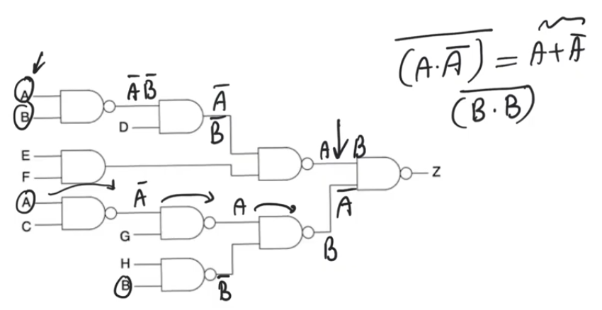
- The circuit expression is
Z=(((AB)'DEF)'.(((AC)'G)'(BH)')', we need to get the input variables other than A that will bring us the glitching structure Z=A+A'
- First
NAND gate has to have B=1 to allow A to propagate
- Then
D=1 to allow A' to propagate through the AND gate
E=1 and F=1 to allow A' to propagate through the NAND gate to prevent them from masking the output to zeroC=1 to allow A to pass through the NAND gate and G=1- Finally either of
H or B has to be equal to 0 to output a 1 from the NAND gate to allow the A to propagate, BH=00,01,10
- But in the top branch we force
B=1, which doesn’t allow us to use any combination except for BH=10
- so the final combination that show the glitch is
ABCDEFGH=X1111110
- The gltich appears because for this combination regardless of the value of
A we should have an output equal to Z=1
- however for this transition we are relying on
A to keep the function equal to 1
- The glitch is removed by adding a product term that’s gonna be
1 for this input variables combination BCDEFGH'
Z=(((AB)'DEF)'.(((AC)'G)'(BH)')'+BCDEFGH'