Defects, faults and errors
Digital IC design and vlsi notes
Defects, faults and errors
- Source this playlist on Testing.
Terminology
- DFT uses alot of terminology,
- some of the words have colloquial uses that are very similar
- but they mean different things in DFT
Testing and Verification
- Testing refers to making sure that a finished chip is working
- Testing usually applied to finished products (fabricated chips)
- this could apply to a prototype, FPGA, research chip
- it’s usually refers to a chip that is shipped for commercial use
- It’s testing the design in a hardware platform,
- if the product is destined for an FPGA, testing the design when it’s actually burnt on the FPGA
- Verification is about the design, you verify the design not the finished product
- Any kind of testing before fabricating the chip is considered fabrication
- All the simulation at whatever level are considered fabication
- Testing usually applied on a per chip basis, evrey chip has to be tested before it’s shipped
- Verification has to be done for the design and it’s done once, but the test is done for every finished product
- If your ultimate platform is an ASIC and you use an FPGA first to test the functionality for example, then using the FPGA to check first is part of verification
- It’s much cheaper to do verification than to do testing
- So you need to expand as much effort as you can into making sure that your design will work once it’s fabricated
Defect, fault, and error
- They describe pretty much the same thing at different levels of abstraction
- A defect is an actual physical problem that happens when we fabricate a chip
- A fault is one way in which we can model this defect at a certain level of abstraction
- An error is an observation that you make when you perform a test that exposes the uderlying fault and defect
Example
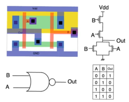
- standard cell entry for a two input nor gate
- layout
- circuit level model (delay, power information)
- logical model
- truth table model
- each of these entries represents a different level of abstraction

- Defects are physical problems, they are the root cause of everything has to be done in DFT
- CMOS fabrication is a very long process and alot of things that can go wrong when applying photolithography
- All of these issues can lead to physically realised problems and deviations on the chip
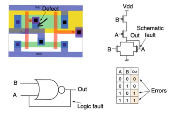
- Assume we have a problem in the layout that leads to a short circuit
- due to misalignment or wrong etching, or overdiposition of metal, or other reason
- this pyhsical manifestation of the problem is called a defect
- A fault model is one way in which we can model this defect at a certain level of abstraction
- There can be different faults that results from the defect
- At the circuit level this over metal deposition can be modeled as a short circuit between the drain and the gate of a transistor (output and input A)
- A schematic fault model of this defect
- It can be modeled at the logic level as the short circuit of between input A and output of the gate
- This is a different fault model for the same defect
- Which model is used for the fault depends on the kind of fault that happened
- An error is a deviation from the gold standard that you see as an observation of a defect
- In the example when the input is (0,0) a 1 should be observed, seeing 0 at the output is an error
- this error indicates that there is a defect underlying this and that this defect can be modeled in one of different ways using the fault models

- Certain defects can manifest themselves in certain fault modeling levels but not in others
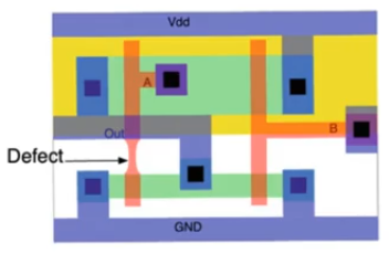
- consider the example’s defect that is due to under deposition or over itching of polysilicon that leads to thinner polysilicon line at a certain location
- If the logic level is used to model this fault then it’s impossible to model it (you’ll have the same logic gate as the correct one)
- because there is no tools at this abstraction level to model what’s happened here
- no errors won’t be observed
- On the other hand if the circuit level is used to model this fault then you’ll observe certain errors
- because the narrowed polysilicon line will have a higher resistance than expected
- so perhaps you’ll see a delay performance that is worse than expected
- so the circuit model can expose this defect into a fault that can reflect into performance
