Scan Technique
Digital IC design and vlsi notes
Scan Technique
- Source this playlist on Testing.
Introduction
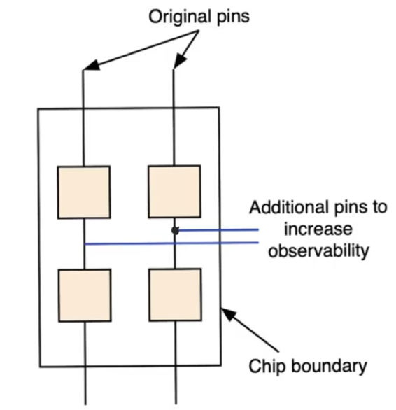
- One major problem that DFT has to deal with is observability and controllability of the internal nodes
- Internal nodes within the chip aren’t reachable for direct control or observation
- If we need to test a specific module within the chip we will need to control its inputs and observe its outputs
- The most naive way to do this is to pull them out to additional pins
- can’t waste too many pins on putting out internal nodes because pins are the most valuable resource
Multiplexing pins
- sharing pins to increase controllability and observability using multiplexers
- Mutliplex pins between test nodes and normal nodes
- A systematic way to do this is using scan technique
Scan Technique
- The scan technique depends on thefact that the majority of our circuits are synchronous pipelines
- They contain combinational logic blocks sandwitched between registers
- The level of granularity that we are dealing with is the level of the combinational logic blocks
- we need to provide full controlability to the inputs of the CLB and full observability to the outputs of the CLB
- regardless of where the CLB is, whether it’s deep in the pipeline or it’s in the periphery
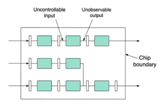
- The way to deal with this is to design a scan register
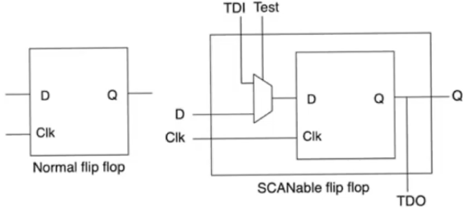
SCAN Flipflop
- Replace every single pipeline register on the design by a scan register
- This is usually handled by the CAD tool
- Additional pins to normal flipflop
TDI: Test data inTDO: Test data outtest: A control pin which indicate whether or not we are in test mode
- It’s a very minor difference and hardware cost, and gives incredible controllability and observability on your circuit
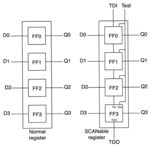
SCAN path technique
SCAN register
- The
test input of each flipflop is connected to a single test input that is provided to the register as a whole
- There are always three additional pins for each register however its size was (
Test,TDI,TDO)
- All of the flipflops in the register share the same
test input
- The
TDI input of the register is provided to the TDI input of the first flipflop in the register
TDO output of the first flipflop is provided to the TDI input of the next flipflop- and so on till the last flipflop of the register which will provide its own
TDO to the external TDO of the register
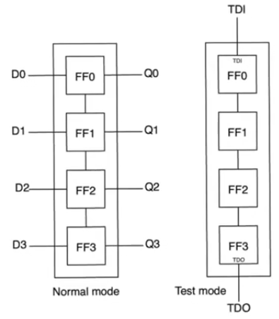
SCANable register modes
- It has two modes
- when
Test=0 normal mode,
- each flipflop passes its
D input to its Q output
- when
Test=1 Test mode,
- the scannable register is functioning as a shift register
- each of the flipflops is gonna accept the
TDI input and passout the TDO output
- There are as many shifts in the register as there are bits in the original register
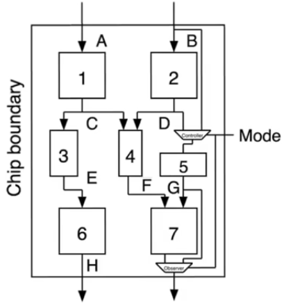
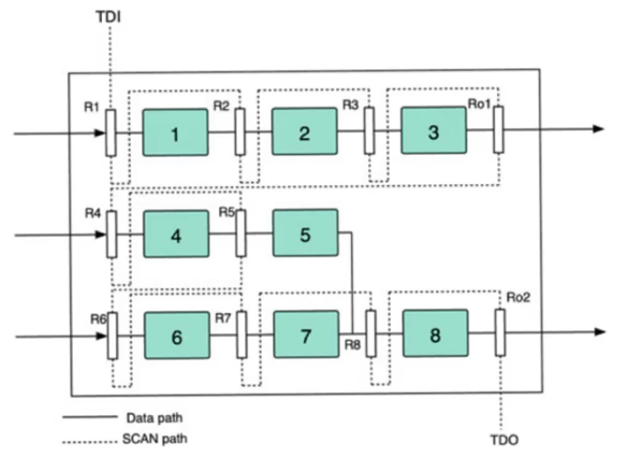
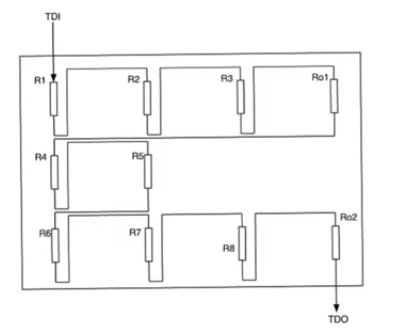
Chip example
- It consists of 8 CLB in a sync pipeline
- The placement and routing tool is gonna route the circuit normally (solid lines), this is the datapath
- There is also an additional path that is created called the SCAN path
- It accepts an input from the chip
TDI external pin
- It routes it so that it becomes the
TDI input of the first register
- Then it takes the
TDO output of the first regiser, routes it so that it becomes the TDI input of the next register and so on
- The dotted line forms a loop throughout the entire chip from the first register
R1 to the last register Ro2 where its own output TDO is gonna be provided to the output pin TDO
- All the registers share a single
Test mode signal, TDI, and TDO
- This setup for testing is only gonna add three pins to the chip
How the test is done
- Set
Test=1 to indicate that we are in test mode
- This causes all the registers to become shift registers
- From
TDI to TDO you observe a very long shift register that includes all the registers on the circuit
- Then we have our test vector prepared
- The test vector is the contents we wish to have in each of the registers
R1 therough R8
- Then start feeding this vector through
TDI, applying cycles
- enough cycles so that the whole test vector shifts through the humongous shift register and settles in all of these registers
- Then switch to
Test=0 normal mode going to the normal operation of the circuit
- All of the registers are operating in parallel feeding their inputs to their CLBs
- Then apply a single clock cycle
- The CLBs will accept the inputs from the registers (the inputs that you put there manually)
- The CLBs are gonna provide outputs to their output registers
- These outputs will be registered at the output registers
- Then swich back to test mode again
Test=1,
- now we have the outputs that we need
- we get the outputs of the internal registers by applying clock cycles so that the contents of the registers shift out to
TDO
- mean while as we are shifting out the outputs from
TDO we can apply a new inputs in TDI
Problem with this method
- The main problem with this is the latency
- The deeper the pipeline the longer the shift registers that you have, and the more cycles that you have to apply to the shift register to shift out the observation vectors
solution
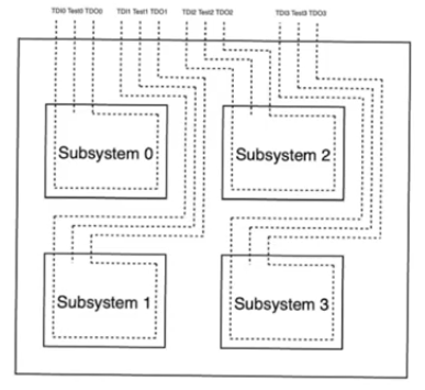
- What we do sometime is that we divide the circuit into subsystems from the point of view of design for testability
- each of these subsystem could have its own
TDI, TDO, Test inputs and its own scan path
- This will shorten the scan path but it comes at the cost of additional pins because you’ll need three additional pins per each module
- we can also mutliplex the inputs of the subsystems to reduce the number of pins and have select lines to choose between the submodules
- The cost here is that we can only test one submodule at at time