Boundry scan and JTAG
Digital IC design and vlsi notes
Boundry scan and JTAG
- Source this playlist on Testing.
Introduction
- JTAG (Joint Test Action Group) is an IEEE standard used to allow designers to use the BST (Boundry scan technique)
- BST is a technique that allows us to probe pin values of chips installed on pcbs without having to use physical probes
- This is analogous to a topic within DFT in microchips
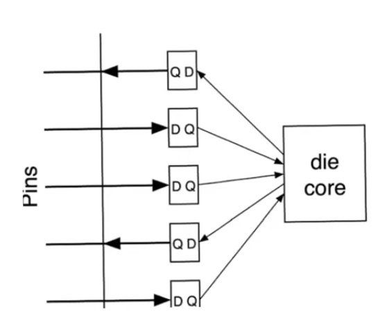
Chip boundry
- Within the IC package there are the chip’s inputs and outputs connected to registers contained within the die
- used to register the values of the pins before they are presented to die or pcb
- These registers would allow communication in parallel
BST
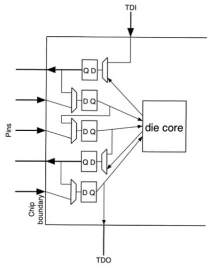
- The boundry scan technique requires us to modify every input and output register in the chip into boundry scan register
- The BST is a scaling up of the scan technique from the chip level to the pcb level
- While most embedded systems designers wouldn’t have to deal with scan technique, they would have to understand the BST
- The two aren’t mutually exclusive,
- you can have the scan technique enabled on the chip
- and BST enable on the PCB and the two aid each other
- The first step is to modify every register into a BST register
- All registers will have an additional multiplexer
- The Mux will feed the
D input of the register either a normal input, or a test input
- The test data input
TDI is different from the TDI in the scan technique
- same for the select
Test input pin that sets the multiplexers in test mode or normal operation mode
- In test mode operation is similar to scan technique,
- the first register will accept the
TDI input
- the second register will accept the registered value (output) from the first register
- and so on till the final register that accepts the output of the previous one, and it provide it’s output to a pin called
TDO
- Test data output
TDO pin is also independent from the TDO in the scan technique
PCB setup with multiple chips
- In a pcb with multiple chips connected with (multibit) copper tracks
- All chips in the PCB are boundry scan compatible (each one have BST modifications)
- each one have
Test, TDI, TDO pins
- There is also
Test, TDI, TDO jacks on the PCB itself
- There are two sets of tracks on the PCB
- The tracks that connect the chips to each other so that they function properly and form a system with each other
- There is an indenpendant set of tracks that form a boundry around all these chips
- The other tracks starts from the
TDI jack goes to the TDI pin of the first chip
- Then exit through
TDO of the first chip
- Then the
TDI of the next one
- till it reaches the last on
- The final chip’s
TDO is connected by track to the TDO jack of the PCB
- The PCB
Test input is also distributed to the Test pin of all chips
BST Usage
- BST is useful when you create a PCB with multiple chips you don’t have mechanical access to the pins (you can’t probe them)
- specially in case of BGA packages
- This allows you to probe the values of the pins because they are all part of a shift register
- You can also force the values of a chip inputs to a specific value
- This can be combined with the scan technique to have nested levels of scanning
- BST also can be used to probe and ensure the integrity of the assembly
- you can ensure that the pins are actually connected to the copper tracks
- it’s also a way to test the pcb itself and the connection of the chips within it
- you can force the output pin of a certain chip to a certain value and then you can check that you received this value properly at the other chips
- The specific way in which you perform a test (how the test vectors are shifted from
TDI to TDO) is specified by the JTAG standard.